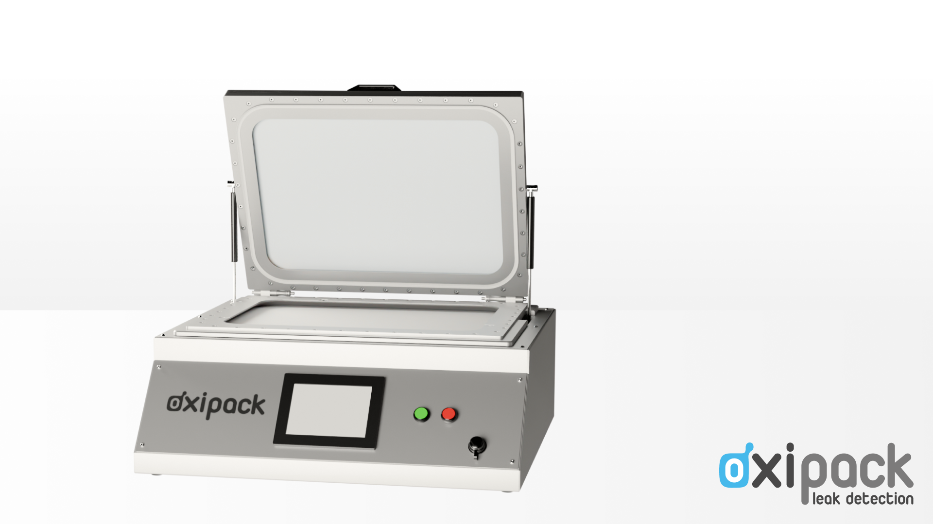
STATIONARY LEAK TESTER R&D (SLT R&D) – OXIPACK
Features:
- Non-destructive vacuum decay method (ASTM F2338).
- Tests both large and micro leaks in a wide range of flexible (MAP) packaging.
- Capable of testing multiple packs or sachets simultaneously for greater efficiency.
- 7” touchscreen for easy operation, quick settings adjustments, and result monitoring.
- Visual indicators (green/red) and precise leakage measurements for immediate, objective results.
Benefits:
- Cost-Effective: Non-destructive method preserves packaging, reducing waste and saving resources.
- Accurate & Reliable: Detects both large and micro leaks with precision for reliable quality control.
- Efficient: Tests multiple packages at once, speeding up the testing process.
- User-friendly: Intuitive touchscreen and visual indicators simplify use and decision-making.
Technical Specifications:
- Dimensions and Weight: 665 x 705 x 333 mm (L x W x H) 40 KG
- Materials: Stainless steel, Anodized aluminium, Polycarbonate, Rubber
- Power Supply: 100 – 230V 50/60HZ
- Air Supply: > 5.5 – < 8 bar / 8mm connection
- Compliance and IP Rating: CE IP20
- Size measuring chamber: 350 x 500 x 116 mm (L x W x H)
- Leak Detection Method: ASTM F2338
- Minimum Leakage: > 0,9 cm3/min
- Maximum Testing Capacity: 2 P/M
- Connections: USB/Ethernet export, 24VDC logic (free programmable)
- Packaging Type and Size: MAP up to 350 x 500 x 116 mm (L x W x H)