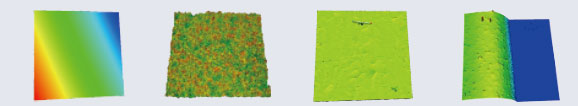
- Measurement function: it can realize high precision Z scanning of sample surface and obtain 3D image.
- Analysis function: It can obtain 2D and 3D data such as surface roughness, micro-nano-level contour size, etc.
- Programming function: Support pre-configured data processing and analysis tool steps, one-click to complete the whole process from measurement to analysis.
- Batch analysis: Data processing and analysis templates can be customized according to the customer demands, and one-click batch analysis can be realized for the same type of parameter data
Details
Application
Semiconductor, polished silicon wafer, thin silicon wafer, wafer IC
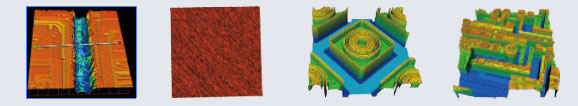
3C electronics, sapphire glass roughness, metal shell mold defects, glass screen height difference
Parameters
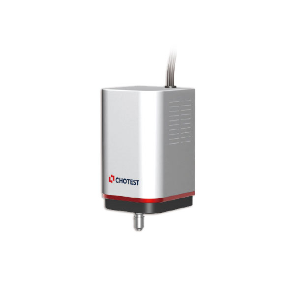
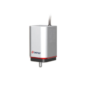
| Model No. | SuperView WX100 | |
| Light Source | White LED | |
| Video System | 1024×1024 | |
| Objective Lens | 10X(2.5X,5X,20X,100X optional) | |
| F.O.V | 0.98×0.98mm(10X) | |
| Lens Turret | Single hole / 3 holes manual | |
| Size | 230×200×380mm | |
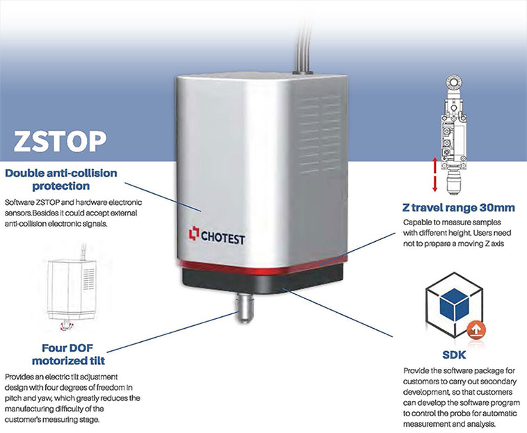
| Tilt | ±2° Motorized | |
| Z Travel Range | 30mm | |
| Z Scanning Range | 10mm(Depend on Lens) | |
| Z Resolution | 0.1nm | |
| Roughness RMS Repeatability*1 | 0.01nm | |
| Step Height Measurement |
Accuracy*2 | 0.5% |
| Repeatability*2 | 0.1% 1σ | |
| Note: *1 Measure Sa 0.2nm silicon wafer in a laboratory environment according to the ISO 25178. *2 Measure standard 5μm steps height block in a laboratory environment according to the ISO 10610-1:2009 |
||